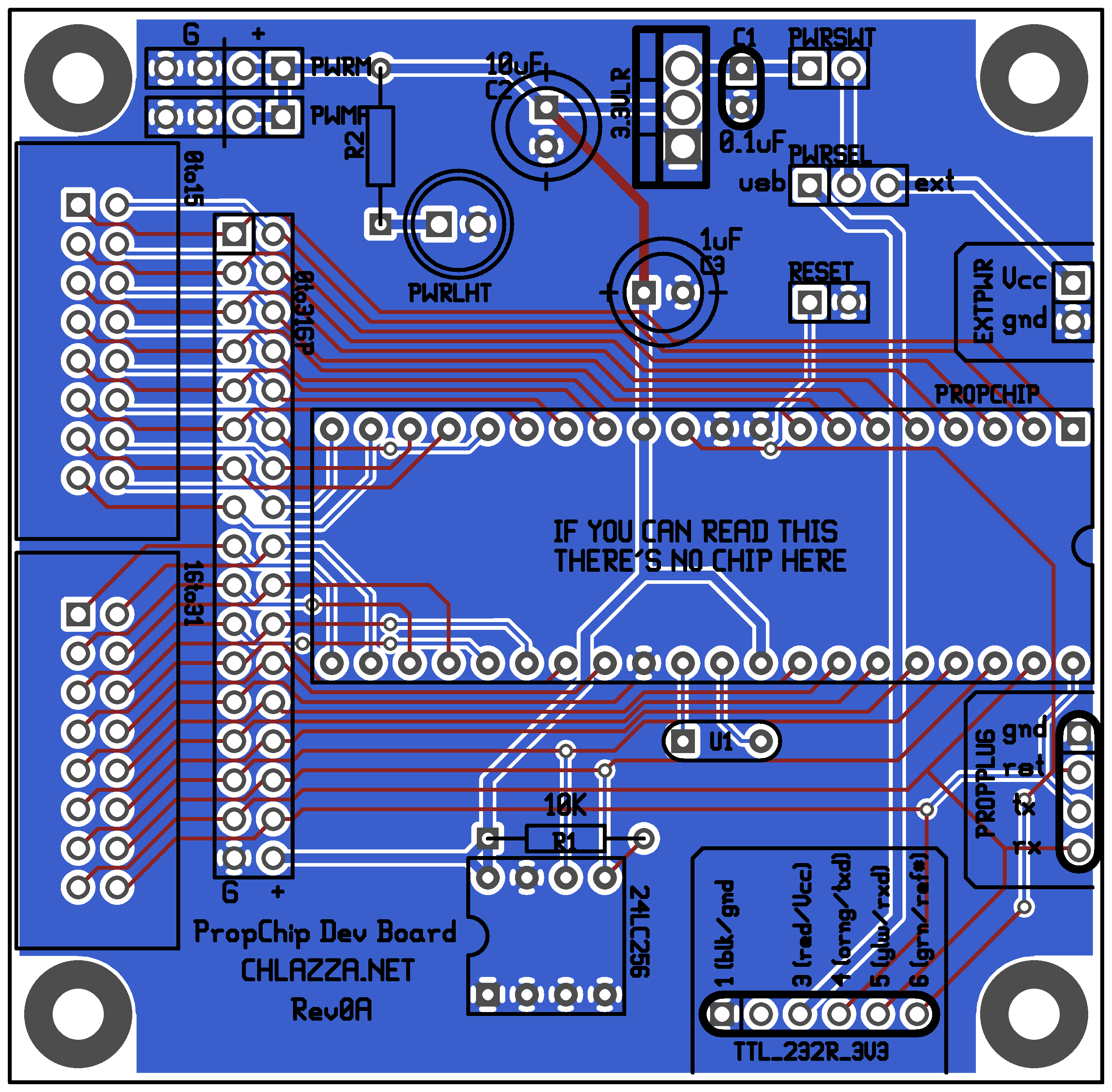
 Rewind the clock a couple of years (2006ish). The only two development boards Parallax manufactured for the Propeller chip were a ~$70 dev board that had just about everything, and a Propeller chip on a perf board that was dirt cheap. I wanted something in between: something that was cheap and universal enough to embed, but designed to be (and could be) reused.
I've been tinkering with the project since. The original layout was in Cadsoft's Eagle utility, but the emulator I was using to run Windows on my workstation got screwed up when Sun bought the company and pushed out a few updates. I had long since bought the parts (2007), and a few weeks ago I decided I was tired of staring at the bag collecting dust on my desk. I whipped up a schematic in an evening and started in on the layout.
Layout (gEDA PCB format): here
M3x0.5 ISO 262 Metric Screw screw footprint (gEDA PCB format): ISO262_M3_screw.fp
Go here to generate arbitary footprints for headers.
Schematic (gEDA gschem format): propchip_devboard_rev0.sch
gEDA gschem FTDI TTL-232R-3V3 cable symbol: ftdi_ttl_232r_6pin_usbcable.sym
gEDA gschem Parallax Propeller Chip symbol: p8x32a_dip.sym
gEDA gschem STMicroelectronics LD1117V33 linear regulator symbol: LD1117V33.sym
gEDA gschem Microchip 24LC512 EEPROM symbol: 24lc512.sym
[2009-08-25]
Got it fabricated and stuffed.
Revision changed; was 0, is now 0A.
Made some header drill holes bigger, shortened the board to reduce cost, moved stuff around.
Files updated.
NOTE: The dual shrouded header footprints at the left side of the board are bad. Despite careful measurement, they are too short and too wide. As such, I can only fit one socket on at a time.