 Okay. *hand wavy motions*
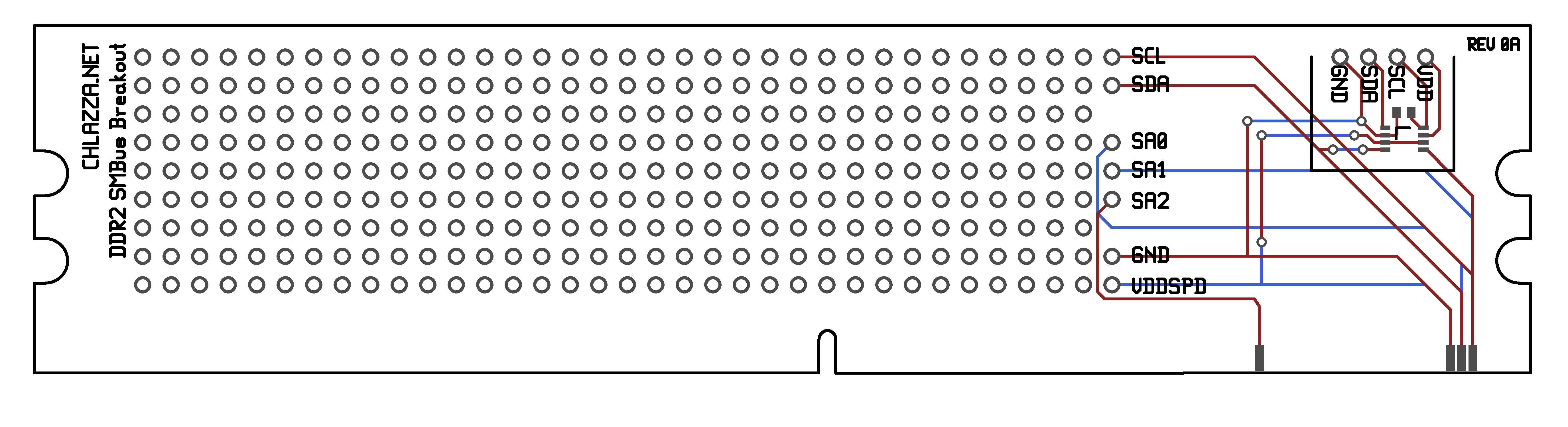
The basic idea is to breakout the SMBus lines of a DDR2 DIMM slot into a perf-board-style prototype board. I took it a step further and added a TI TXS0102 level shifter to the SCL and SDA lines. This will protect the mainboard to some degree (hopefully), allow higher voltage devices to be attached to the bus, and to work around the somewhat limited current supply to the DIMM. (I think JEDEC specs indicate a max current draw of a few dozen milliamps?)
NOTE: As I understand it RAM is supplied with voltages lower than the traditional computer 'low voltage' of 5VDC - however, on the specs from JEDEC, the EEPROM on the DIMM is provided with its own voltage supply - VDDSPD - so I'm honestly not sure WHAT the SMBus there is running on. The first thing I plan to do when I fab a board is to put a voltmeter on the VDDSPD and GND pins and see whats coming out.
WARNING: If the VDDSPD voltage turns out to be something like 5VDC, this will damage the level shifter I selected! The A port on the TXS0102 only supports 0VDC (well, -0.5VDC) to 4.6VDC. Also, the supply voltage for B port MUST be equal to or higher to the supply voltage for A port. So says the level shifter datasheet at any rate.
The extra 0603 outline above the shifter is for a pull-down resistor - when either of the Vcc ports is low on the shifter, it shuts down. Adding the pull-down makes sure the device isn't floating and messing with the bus if nothing is connected to it.
The prototype area to the left is a simple 100 mil grid of holes.
The JEDEC docs also indicate several lines connected to the address pins of the EEPROM. Is most applications I've seen, these pins are connected to ground. Didn't know if they would be useful or not, so I broke them out anyway.
Now, while simple in theory, the devil is in the details.
By far the hard part of this project was the DIMM and contact pad layout since it needs to be ex-fucking-zact. It took me a while to locate the official JEDEC measured drawings - I actually got my measurements off of a DIMM socket datasheet I got off of Digikey.
The SM8 footprint of the level shifter was also a pain - getting everything measured up and laid out correctly took about a day.
[2009-06-10 1153]
Got my laser printer back.
Turns out the alignment notch was off by ~1mm. I fixed that, and then discovered that the board width/length/whatever may be wrong as well. It MAY be within tolerance (as defined by Molex at least), but once I get that fixed I'll upload the corrected files and send it off to get fabbed.
[2009-06-10 1205]
Nevermind, its spot on at 133.35mm!
Files updated.
[2009-07-09]
Got the board back from BatchPCB.
I screwed up, made most of holes too small:
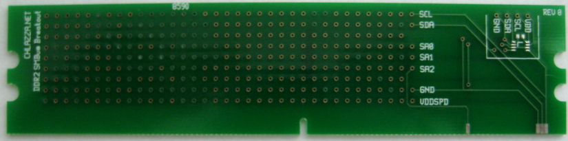
Whoops. Good enough for a test board, but it isn't going to work as a perf board. Oh well! That's why it's revision zero!
[2009-08-25]
Revision change; went from 0 to 0A.
Only change was that the hole diameter was bumped up to 38 mils.
Files updated.
[2009-09-21]
BatchPCB delivers a board that is too thick for DDR2 DIMM slots apparently; my board is ~1.5mm (0.062"?) and the Molex datasheet lists 1.27(+/-0.10)mm (0.05") for board thickness.
Oops. (TIWIIRZ!)
I discovered this while attempting to force my prototype board into a spare DIMM socket on a Gigabyte mainboard.
This presents a bit of problem because board thickness doesn't seem to be a variable that PCB fab companies want to adjust. (For very low volume orders at any rate.)
